Main features
Three functions in one
- Mass storage flashing (MSC) – copy
.bin/.hexfiles to program Flash. - Virtual COM port (CDC) – log output and interactive console without a separate USB‑UART dongle.
- CMSIS‑DAP debugging – works as a standard CMSIS‑DAP probe for breakpoints and memory access.
Integration‑friendly hardware
- USB‑C as the only host connector – power + data for SWD/JTAG in a single cable.
- Board‑edge headers let you route SWD and UART into your own main boards.
- On‑board regulation and protection suitable for common 3.3 V Cortex‑M targets.
Open ecosystem · CMSIS‑DAP standard
- Built on the open source Arm Mbed DAPLink project.
- Standard CMSIS‑DAP protocol – not tied to a single MCU vendor.
- Interface firmware can be rebuilt to support more targets or custom features.
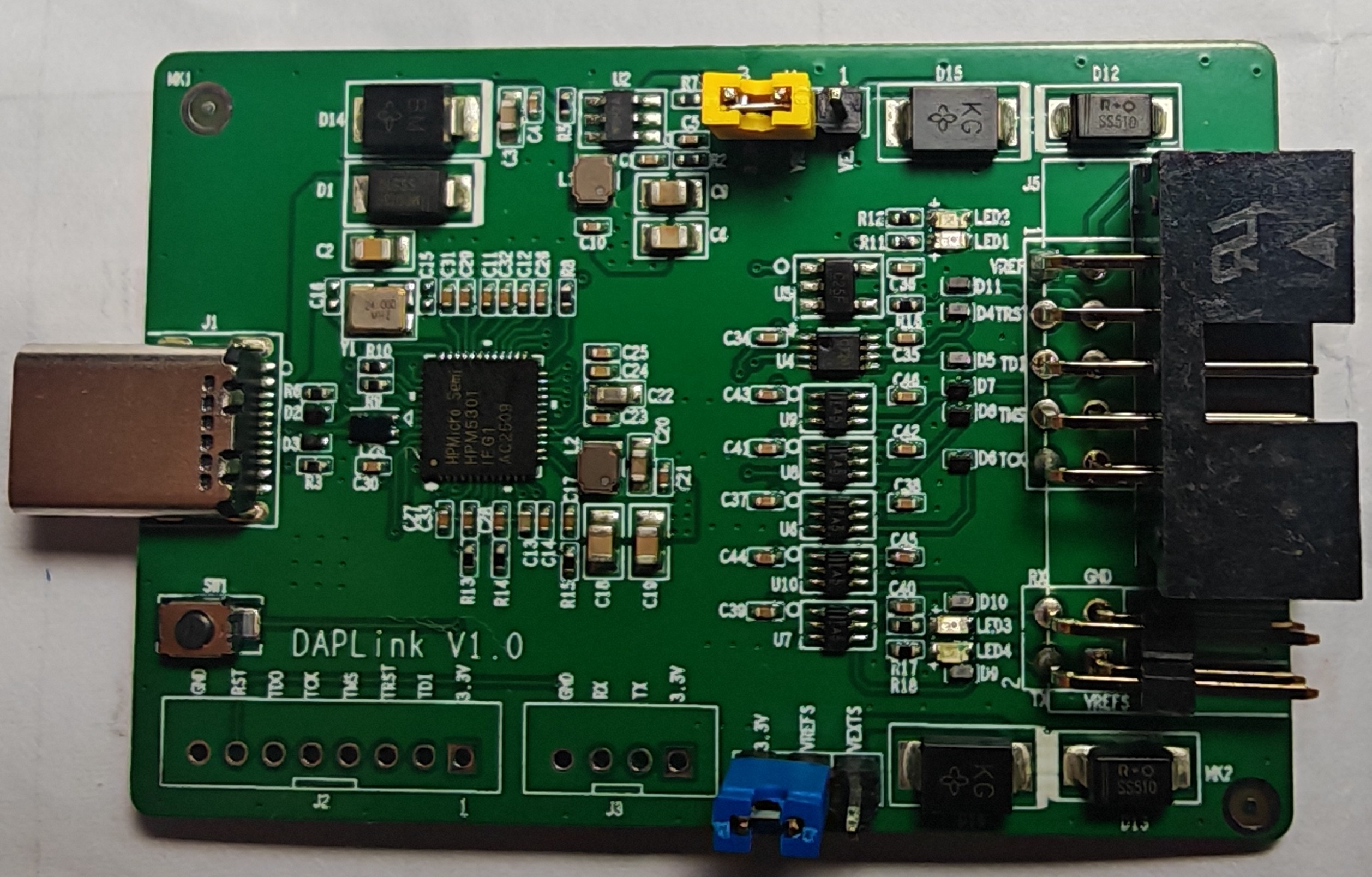
Hardware overview
| Item | Details |
|---|---|
| Interface MCU | ARM Cortex‑M MCU running DAPLink interface firmware (e.g. LPC / STM32 class). |
| PC connection | USB Type‑C; 5 V power and data. |
| Target interfaces | SWD/JTAG debug header + UART header (TX/RX/GND, 3.3 V logic). |
| Power | 5 V from USB‑C, on‑board regulators; VREF pin to sense target I/O voltage (typically 2.3–3.3 V). |
| Indicators | Multiple LEDs for DEBUG status, VREF monitor and power diagnostics. |
| Firmware update | On‑board button to enter bootloader – update DAPLink interface firmware when needed. |
| Form factor | Compact PCB ready to fit into a small enclosure (see case rendering). |
Connectors & signals
DEBUG header (SWD / JTAG)
- Typical pins: TCK/SWCLK, TMS/SWDIO, TDI, TDO, nRESET, VREF, GND.
- Used for on‑chip debugging, Flash programming and production test.
UART header
- Signals: TX, RX, GND, 3.3 V.
- Acts as a console port for the target – ideal for logging and shell access.
Buttons / jumpers
- Button to enter bootloader / reset the interface MCU (exact behavior depends on firmware build).
- Jumpers can configure target power feed or mode, according to the final PCB design.
Quick start
1
Hook up the hardware
- Connect DAP‑LINK to your PC with a USB‑C cable.
- Connect the DEBUG header to the target SWD/JTAG header; connect UART if needed.
- Make sure target power and VREF voltage match (usually 3.3 V).
2
Drag‑and‑drop flashing
- A new USB drive appears on your PC (name depends on the firmware build).
- Copy your compiled
.bin/.hexfile to that drive. - DAP‑LINK programs the target MCU flash automatically.
3
Serial log & debugging
- A virtual COM port is exposed – open it in your favorite terminal to see logs.
- In Keil / pyOCD / OpenOCD select the CMSIS‑DAP device and start source‑level debugging.
FAQ
Which tools are supported?
Any debugger that speaks CMSIS‑DAP: Keil MDK, Arm DS, pyOCD, some OpenOCD configurations, and VS Code setups using CMSIS‑DAP backends.
How is this different from ST‑LINK / J‑LINK?
DAP‑LINK is built on open source DAPLink and the CMSIS‑DAP standard, not locked to a single vendor. It is a good fit as a generic debug head for your own boards or product lines.
Can I customize or replace the firmware?
Yes. The interface MCU can be updated with different DAPLink builds so you can support new targets or add features as needed.